8. Nanometer-resolution white-light scanning interferometry for surface-profiling of hybrid bonding samples for advanced semiconductor packaging
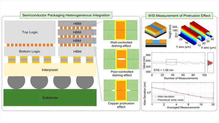
Recent advancements in semiconductor three-dimensional (3D) packaging ignited the need for higher-precision surface metrology, especially for hybrid bonding. This study addresses the technological strength of white-light scanning interferometry (WSI) over atomic force microscopy (AFM) and confocal laser scanning microscopy (CLSM) for nano-meter-resolution hybrid bonding surface measurements/inspections. Two exemplary hybrid bonding samples were prepared for this comparative test with different chemical mechanical polishing (CMP) treatments – one maintaining a metallic tantalum thin-film and the other having an over-polished lower dielectric Tetraethyl Orthosilicate (TEOS) layer without tantalum thin-film, mimicking the copper protrusion. The same samples were measured by WSI and CLSM; the results were compared with the contact-type AFM measurement, the golden standard method in the industry. WSI reconstructed the surface profile similarly to the AFM and showed sub-nm repeatability with a standard deviation of 0.79 nm after 20 consecutive measurements, further supported by the Allan deviation analysis, proving that the system is not affected by non-stationary noise. Interestingly, the existence of a thin film does not affect the stability of the WSI system. CLSM could not appropriately reconstruct the surface profile, and repeatability was also evaluated to be lower than that of WSI. With the proper knowledge of the TEOS and Silicon Nitride thickness, through precision calculation of the phase spectrum change in Cu and Silicon Nitride, we can reconstruct the surface profile with high precision. Theorical analysis and Finite-Difference Time Domain (FDTD) simulation were also conducted for in-depth understanding about phase change effect on hybrid bonding sample. Based on these theories and simulations, the universality and sub-nm level accuracy of optical metrology for various bonding materials were verified.
Sukkyung Kang
My research focuses on the phenomena arising from the physical contact between two engineered surfaces. The goal is to develop processing technologies that can create high-value, innovative products by precisely manipulating phenomena such as friction, wear, polishing, bonding, diffusion, adhesion, and deformation.