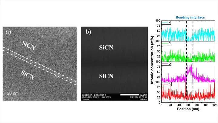
To enhance the density and performance of semiconductor devices, 3D packaging with hybrid Cu bonding is emerging as a critical technology. One of the dielectrics used in hybrid Cu bonding is SiCN, typically deposited using PECVD (plasma-enhanced chemical vapor deposition). In this study, we investigated SiCN deposited at room temperature using PVD (physical vapor deposition). The SiCN, with a thickness of 150 nm, exhibited a surface roughness of 0.3-0.4 nm after the CMP (chemical mechanical polishing) process and a contact angle of about 10 degrees and dielectric constant of 3.9, indicating its potential as a dielectric for hybrid Cu bonding. And, PVD SiCN-SiCN bonding was performed at 260?C, resulting in a uniform and void-free interface.
Sukkyung Kang
My research focuses on the phenomena arising from the physical contact between two engineered surfaces. The goal is to develop processing technologies that can create high-value, innovative products by precisely manipulating phenomena such as friction, wear, polishing, bonding, diffusion, adhesion, and deformation.