11. Frequency-comb-referenced Terahertz Fabry-Pérot interferometry for monitoring semiconductor wafer thinning process with a nanometer precision
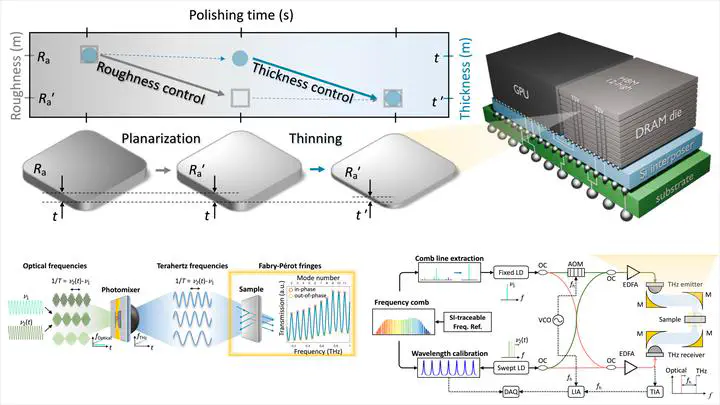
High-precision, non-destructive thickness measurement is essential in semiconductor manufacturing. Optical methods often struggle with strong surface scattering and absorption during wafer thinning. We present nanometer-precision, non-destructive wafer thickness measurement using the absolute frequency positions of Fabry-Pérot interference modes in the terahertz frequency regime, referenced to a frequency comb. By leveraging the comb’s SI-traceable frequency uncertainty and terahertz radiation’s scattering insensitivity, this approach achieves a 58.4-nm precision in 0.2-s and 7.2-nm in 25.6-s averaging. Such unprecedented performance enables effective monitoring of wafer thinning processes (e.g., chemical mechanical polishing), crucial for advanced semiconductor packaging.
Sukkyung Kang
My research focuses on the phenomena arising from the physical contact between two engineered surfaces. The goal is to develop processing technologies that can create high-value, innovative products by precisely manipulating phenomena such as friction, wear, polishing, bonding, diffusion, adhesion, and deformation.